Power Management Technology

Technology

Capacitor-based Power Conversion

Our Story:
pSemi’s journey in capacitor-based power conversion began with the acquisition of the pioneering MIT start-up Arctic Sand in 2017. Arctic Sand understood that using capacitive energy transfer, rather than more traditional inductive switching converters, would establish higher power conversion efficiency in low-profile form factors previously thought unobtainable.

pSemi has continuously developed architectural innovation combined with the latest advances in Murata capacitor technology. This combination has resulted in the release of a wide range of industry-leading products and over 250 patents….and growing!

Unleashing the Power of Capacitive Energy Transfer – the Next Chapter

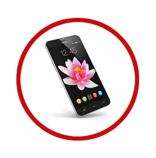
pSemi capacitor-based power conversion technology is now becoming the de-facto standard in multiple applications from mobile smartphones to networking and telecoms. This leadership is evident in the compatibility with standards implementations, such as USB programmable power supply (USB_PPS) and Qi wireless charging implementations, where charge pump technology provides significant efficiency and size benefits when powered from a regulated voltage source.

pSemi offers industry-leading products, including charge pump switched capacitor converters, 2-stage buck and boost (LED drivers) converters, and multi-level converters.

Our Patented Capacitor-based Power Conversion Technologies

Charge Pump Switched Capacitor Converters​

pSemi’s novel charge pump architectures use a small output inductance, acting as a constant current source, to eliminate or reduce capacitive switching redistribution losses. This lossless or adiabatic technique enables higher conversion efficiencies with 20-30% reduction in flying capacitor size and reduced EMI emissions. 

Charge pump, switched capacitor

2-Stage Regulators

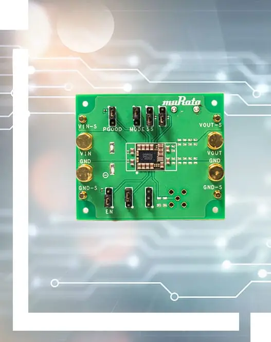
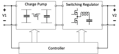
The 2-stage architecture combines charge pump technology with a switching regulator to improve power conversion efficiency in low-profile applications. In the 2-stage buck converter, a charge pump divider is followed by a buck regulator. In the 2-stage boost converter for LED driver applications, a boost converter is followed by a capacitive multiplier.

2-stage buck architecture—a charge pump divider followed by a buck regulator

Multi-level Buck Regulators

At pSemi, we are applying our extensive knowledge and experience in switching capacitor technology to the development of leading-edge, multi-level architectures. 3- and 4-level conversion achieves high efficiency power conversion while reducing the height and size of the output inductor to provide a low-profile solution.

Multi-level buck converter with N-levels of conversion

Contact us to learn more about the latest innovations in multi-level power conversion and product availability.

Enables Next-generation Power Conversion Applications and Delivers the Highest Conversion Efficiency in Space-constrained Applications

Notebook/Laptop
Robotics
Tablet/Phablet
Data Center and High-performance Computing
Smartphone
AR/VR Headset
Home Appliance Automation
E-mobility

Markets

Power Management

Markets

  • High Linearity RF Switches

    Industry-leading linearity and RF performance
    HaRP™ technology enhancement reduces gate lag and insertion loss drift
    Monolithic CMOS solution that integrates RF, analog and digital
    Best-in-class ESD and reliability
  • High Isolation RF Switches

    Industry-leading isolation and RF performance
    HaRP™ technology enhancement reduces gate lag and insertion loss drift
    Monolithic CMOS solution that integrates RF, analog and digital
    Best-in-class ESD and reliability
  • Low Insertion Loss RF Switches

    Industry-leading insertion loss and RF performance
    HaRP™ technology enhancement reduces gate lag and insertion loss drift
    Monolithic CMOS solution that integrates RF, analog and digital
    Best-in-class ESD and reliability
  • Antenna Tuning Switches

    Industry-leading RF power handling and ruggedness
    Best-in-class harmonic and linearity
    Small form factor with robust ESD and reliability
  • 75Ω Wired Broadband Switches

    Unmatched linearity performance for DOCSIS 3.1
    HaRP™ technology enhancement reduces gate lag and insertion loss drift
    Monolithic CMOS solution that integrates RF, analog and digital
    Best-in-class ESD ratings and reliability
  • Broadband RF Switches

    Wideband support with a frequency range from 0 Hz to 67 GHz
    Industry-leading insertion loss, isolation, linearity and settling time
    HaRP™ technology enhancement reduces gate lag and insertion loss drift
    Best-in-class ESD and reliability
  • High Power Switches

    Industry-leading power handling and RF performance
    HaRP™ technology enhancement reduces gate lag and insertion loss drift
    Monolithic CMOS solution that integrates RF, analog and digital
    Best-in-class ESD and reliability
  • Automotive Switches

    AEC-Q100 Grade 2-certified supporting temperatures up to +105°C
    HaRP™ technology enhancement reduces gate lag and insertion loss drift
    Monolithic CMOS solution that integrates RF, analog and digital
    Best-in-class ESD and reliability
  • Extended Temperature RF Switches

    Wide temperature range support from -55°C to +125°C
    HaRP™ technology enhancement reduces gate lag and insertion loss drift
    Monolithic CMOS solution that integrates RF, analog and digital
    Best-in-class ESD and reliability
  • 75Ω Wired Broadband RF Digital Step Attenuators

    High linearity, fast switching time with wide bandwidth
    Best-in-class attenuation error with fine attenuation steps
    Monolithic CMOS solution that integrates RF, analog and digital
    Excellent ESD protection and reliability
  • Glitchless RF Digital Step Attenuators

    High linearity, fast switching time with wide bandwidth
    Best-in-class attenuation error with fine attenuation steps
    Monolithic CMOS solution that integrates RF, analog and digital
    Excellent ESD protection and reliability
  • General-purpose RF Digital Step Attenuators

    High linearity, fast switching time with wide bandwidth
    Best-in-class attenuation error with fine attenuation steps
    Monolithic CMOS solution that integrates RF, analog and digital
    Excellent ESD protection and reliability
  • 2.4 GHz IoT FEMs

    Industry-leading monolithic Wi-Fi RF front-end solutions
    High linearity performance for Wi-Fi 6 and W-Fi 6E
    Compact form factors integrating high-performance RF, analog and digital
    Best-in-class ESD and reliability
  • Phase Shifters

    Ideal solutions for optimizing transmission phase angle
    Low root-mean-square (RMS) phase and amplitude error with fine phase resolution
    Digital control interface with parallel and serial programming options
    Best-in-class ESD and reliability
  • Monolithic Phase & Amplitude Controllers (MPACs)

    Reliable phase and amplitude control for next-generation communications
    Monolithic CMOS solution that integrates RF, analog and digital
    Integrated solution for Doherty power amplifier optimization (MPAC–Doherty)
  • Digital Tunable Capacitors (DTCs)

    Small form factor with high Q
    Monolithically integrated impedance tuning solution
    Wide-band tuning coverage, minimum mismatch losses, high linearity and fast switching speed
    Best-in-class ESD and reliability
  • Power Limiters

    Highly integrated solutions, smaller and more reliable than PIN-diode solutions
    Adjustable threshold control for maximum design flexibility
    High power handling and linearity required for wide-dynamic-range designs
    Fast response and recovery times for instantaneous protection and rapid return
  • Prescalers

    Exceptional performance with high-frequency support up to 13.5 GHz
    Low phase noise performance and low power consumption solutions
    Bare-die solutions for a wide variety of compact high-performance applications
    Best-in-class ESD and reliability
  • Mixers

    Broadband quad MOSFET array cores for high performance
    Industry-leading linearity, isolation and low conversion loss
    Available in MSOP, DFN and QFN packages
    Best-in-class ESD and reliability
  • Switch LNA

    Integrates dual-channel LNA with bypass function & high-power switch
    20W average RF input power
    Low noise figure of 0.9 dB
    +105°C operating temperature

Power Management

RF Mixers & Limiters

Front End Modules

RF Phase & Amplitude Control

Skip to content